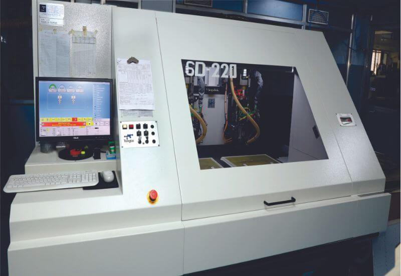
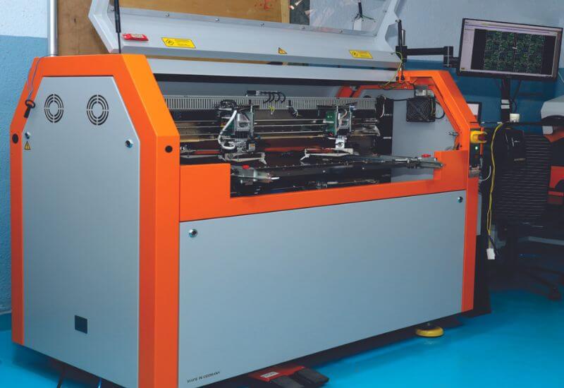
Plant Capabilities
We are equipped with state-of-the-art infrastructure and technologically advanced machines to empower us in solving the most complex requirements of clientele. Our manufacturing plant spans over the XXX sq. m. We utilize machineries and raw materials that comply with international standards such as IPC4101 & IPC-CF-150E. We also possess quality maintenance systems, and availed certifications from the international certification bodies such as ISO. Our plant has extensive capabilities to manufacture multilayer PCBs for telecommunication products, oil & gas applications, military electronics, and others.
Our Plant
Our Plant Capability

Cnc Machine

Photo Printing Machine

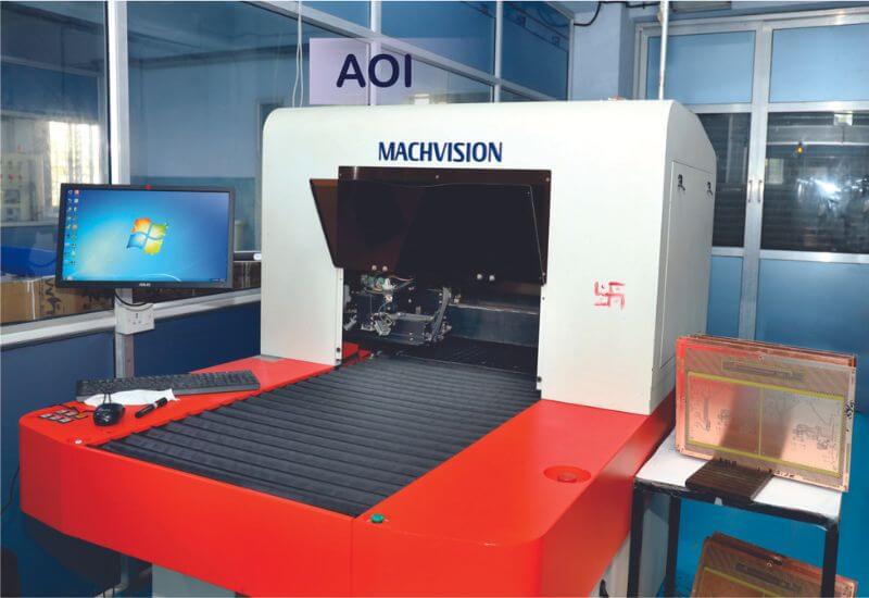
Automatic Optical Inspection

Flying Probe Testing Machine

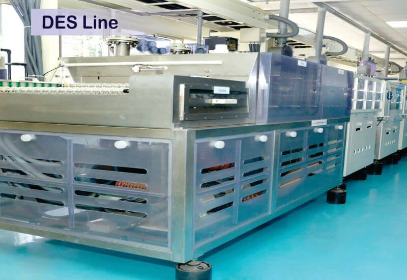
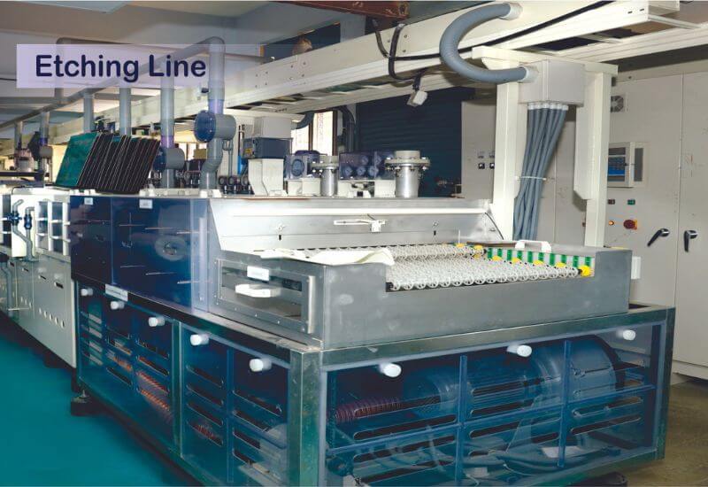
Develop Etch Strip Line

Screen Printing Machine
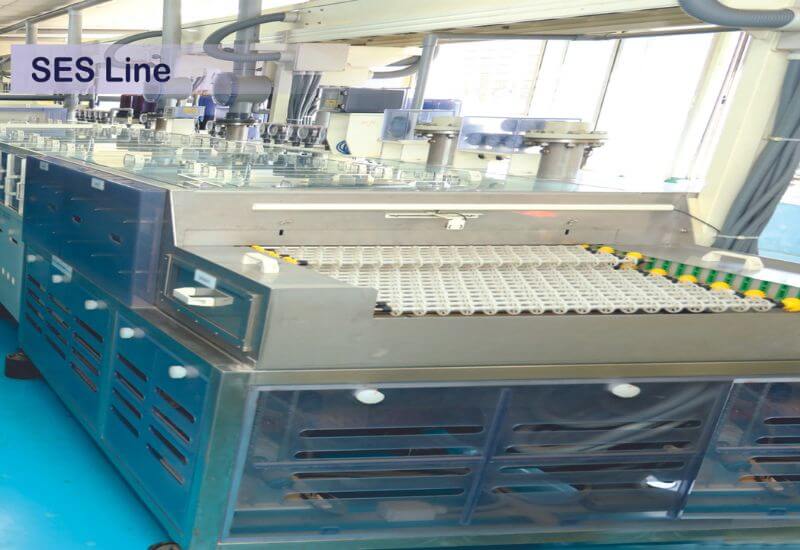
Scrubbing Machine

Impedance-testing-machine
Standard Materials
All Laminate & Prepregs as per IPC4101 & IPC-CF-150E, All Raw Material Nema grade, FR-4, 94V-1, Material used: – Multifunctional Glass Epoxy FR4 (Tg 135), FR4 (Tg >150), FR4 (TG>170).
Approvals & QMS
PCB Fabrication & inspection as per IPC-6012A, Class 2, AQL 0.25, and General inspection level II, Company is ISO 9001-2008 Certified.
PCB Manufactured for
Industrial Controls / Process Automation, Automobile Electronics, Computers / Peripherals / DataComm, Telecommunications products, Scientific and Biomedical equipment, Military and Aviation Electronics.
Our Plant
High Lights Of Plant Facilities
- Full fledged CAM facility.
- Polar instrument for Control Impedance Layer stack up generation software & impedance testing.
- AOI (Automated Optical Inspection) System – In-house Automated Optical Inspection facility for Photo tool, all Inner Layers & outer Layer inspection. Machine from Machvision Taiwan.
- 0.1 mm. CNC drilling capability, Machine from Tong Tai Taiwan.
- Pulse rectifier to achieve uniform Copper Plating thickness on surface & hole wall.
- CMI make hole wall CU thickness & Surface CU thickness instruments.
- PLASMA machine from Jesagi-Hankook Korea – Latest Technology for De-smear etch-back & surface cleaning.
- Flying Probe Tester with 8 probes from ATG Germany.
- Laboratory for process monitoring.
- Microsection facility, Equipment from MEIJI-Japan, Camera with PC interface software.
- Solderability tester.
- DM Water Plant – 100% water usage in process is DM water. Safety/Environmental Full-time IEPA Class ‘K’ Licensed Chemist Ion Exchange wastewater processing.
Our Plant
Final Finishes
- Photoimageble Solder mask On Bare Copper with RoHS Compliant Boards
- Electro less Nickel-Gold (ENIG)
- Lead Free Hot Air Leveling
Final Finishes
As per standard | IPC-SM-840, Class III, type B. |
Photoimageble | Green, Blue, Red, Black, White & Clear as per IPC-SM-840 |
Component Idents | White, Yellow, Black |
Peel able Mask | Blue or Red |
Solder mask Thickness Min. | 10 micron |
Solder mask Dam Min. | 3 mil {0.75 mm} |
Solder mask Clearance | > 1 mil |
Board Dimensions
As per standard | IPC-SM-840, Class III, type B. |
Photoimageble | Green, Blue, Red, Black, White & Clear as per IPC-SM-840 |
Component Idents | White, Yellow, Black |
Peel able Mask | Blue or Red |
Solder mask Thickness Min. | 10 micron |
Solder mask Dam Min. | 3 mil {0.75 mm} |
Solder mask Clearance | > 1 mil |
Copper Cladding
Inner Layer Max Base Cu Thickness | 4 oz {0.14 mm} |
Inner Layer Min Base Cu Thickness | ½ oz {0.017 mm} |
Outer Layer Max Base Cu Thickness | 4 oz {0.14 mm} |
Outer Layer Min Base Cu Thickness | 1/3 oz {0.012mm} |
Aspect Ratio (Thickness to Drill) | 16:1 for 1.6 mm and 12:1 |
Copper Plating | Minimum 0.001” {25 Micron} with hardness of 150 Knoop Maximum |
Min. track/Space | 3/3 mil with base copper 1/3 & ½ oz4/4 mil with base copper 1/3, ½ & 1 oz 5/5 mil with base copper 1/3, ½, 1 & 2 oz 6/6 mil with base copper 1/3, ½, 1 & 2 oz |
Impedance Tolerance Min. | +/-10% {Impedance stack-up design & verification Service} |
Thermal Stress Test | 288 Deg. Centi. 10 sec. One shot |
Flammability | 94V-0 |
Drill Hole Diameter Max. | Unlimited |
Drill Hole Diameter Min. | 0.15 mm {6mil} |