Capabilities
Our Plant
Our Plant Capability

Cnc Machine

Photo Printing Machine
Automatic Optical Inspection
Flying Probe Testing Machine
Develop Etch Strip Line
Screen Printing Machine
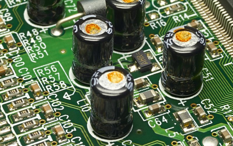
Scrubbing Machine
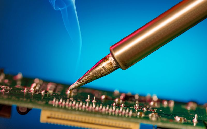
Impedance-testing-machine
Standard Materials
All Laminate & Prepregs as per IPC4101 & IPC-CF-150E, All Raw Material Nema grade, FR-4, 94V-1, Material used: – Multifunctional Glass Epoxy FR4 (Tg 135), FR4 (Tg >150), FR4 (TG>170).
Approvals & QMS
PCB Fabrication & inspection as per IPC-6012A, Class 2, AQL 0.25, and General inspection level II, Company is ISO 9001-2008 Certified.
PCB Manufactured for
Industrial Controls / Process Automation, Automobile Electronics, Computers / Peripherals / DataComm, Telecommunications products, Scientific and Biomedical equipment, Military and Aviation Electronics.
Our Plant
High Lights Of Plant Facilities
- Full fledged CAM facility.
- Polar instrument for Control Impedance Layer stack up generation software & impedance testing.
- AOI (Automated Optical Inspection) System – In-house Automated Optical Inspection facility for Photo tool, all Inner Layers & outer Layer inspection. Machine from Machvision Taiwan.
- 0.1 mm. CNC drilling capability, Machine from Tong Tai Taiwan.
- Pulse rectifier to achieve uniform Copper Plating thickness on surface & hole wall.
- CMI make hole wall CU thickness & Surface CU thickness instruments.
- PLASMA machine from Jesagi-Hankook Korea – Latest Technology for De-smear etch-back & surface cleaning.
- Flying Probe Tester with 8 probes from ATG Germany.
- Laboratory for process monitoring.
- Microsection facility, Equipment from MEIJI-Japan, Camera with PC interface software.
- Solderability tester.
- DM Water Plant – 100% water usage in process is DM water. Safety/Environmental Full-time IEPA Class ‘K’ Licensed Chemist Ion Exchange wastewater processing.
Our Plant
Final Finishes
- Photoimageble Solder mask On Bare Copper with RoHS Compliant Boards
- Electro less Nickel-Gold (ENIG)
- Lead Free Hot Air Leveling
Final Finishes
| As per standard | IPC-SM-840, Class III, type B. |
| Photoimageble | Green, Blue, Red, Black, White & Clear as per IPC-SM-840 |
| Component Idents | White, Yellow, Black |
| Peel able Mask | Blue or Red |
| Solder mask Thickness Min. | 10 micron |
| Solder mask Dam Min. | 3 mil {0.75 mm} |
| Solder mask Clearance | > 1 mil |
Board Dimensions
| As per standard | IPC-SM-840, Class III, type B. |
| Photoimageble | Green, Blue, Red, Black, White & Clear as per IPC-SM-840 |
| Component Idents | White, Yellow, Black |
| Peel able Mask | Blue or Red |
| Solder mask Thickness Min. | 10 micron |
| Solder mask Dam Min. | 3 mil {0.75 mm} |
| Solder mask Clearance | > 1 mil |
Copper Cladding
Inner Layer Max Base Cu Thickness | 4 oz {0.14 mm} |
Inner Layer Min Base Cu Thickness | ½ oz {0.017 mm} |
Outer Layer Max Base Cu Thickness | 4 oz {0.14 mm} |
Outer Layer Min Base Cu Thickness | 1/3 oz {0.012mm} |
Aspect Ratio (Thickness to Drill) | 16:1 for 1.6 mm and 12:1 |
Copper Plating | Minimum 0.001” {25 Micron} with hardness of 150 Knoop Maximum |
Min. track/Space | 3/3 mil with base copper 1/3 & ½ oz4/4 mil with base copper 1/3, ½ & 1 oz 5/5 mil with base copper 1/3, ½, 1 & 2 oz 6/6 mil with base copper 1/3, ½, 1 & 2 oz |
Impedance Tolerance Min. | +/-10% {Impedance stack-up design & verification Service} |
Thermal Stress Test | 288 Deg. Centi. 10 sec. One shot |
Flammability | 94V-0 |
Drill Hole Diameter Max. | Unlimited |
Drill Hole Diameter Min. | 0.15 mm {6mil} |
