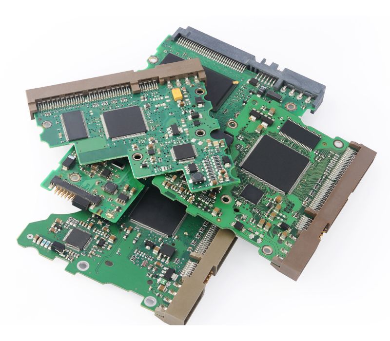
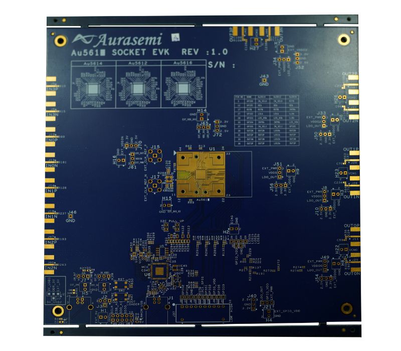
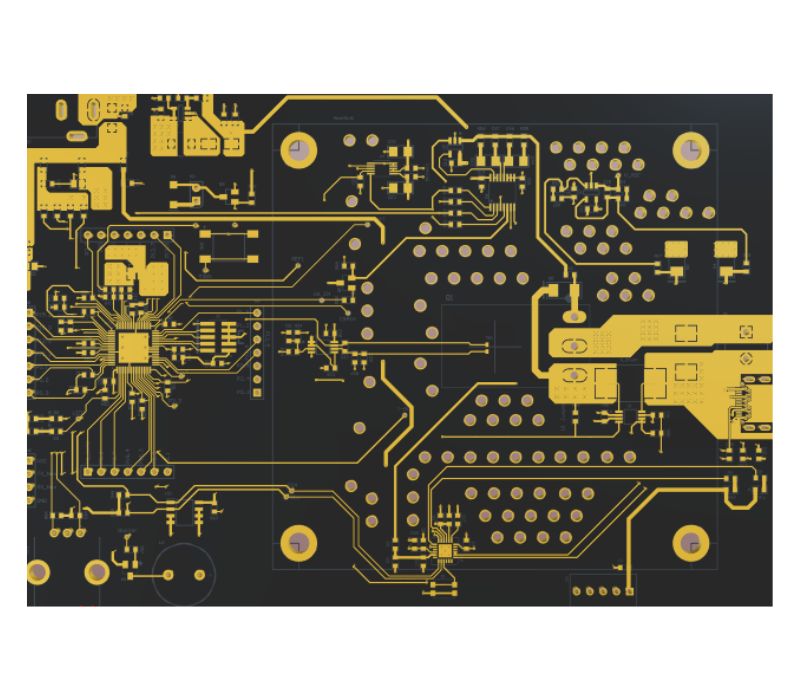
Edge Plating Boards
Electroplate Walls are connected with two pads on the Top & bottom layer. Contact Us
Electroplate Walls are connected with two pads on the Top & bottom layer. Contact Us
Via is plugged with solder masked via for to complete filled non-conductive via. Contact Us
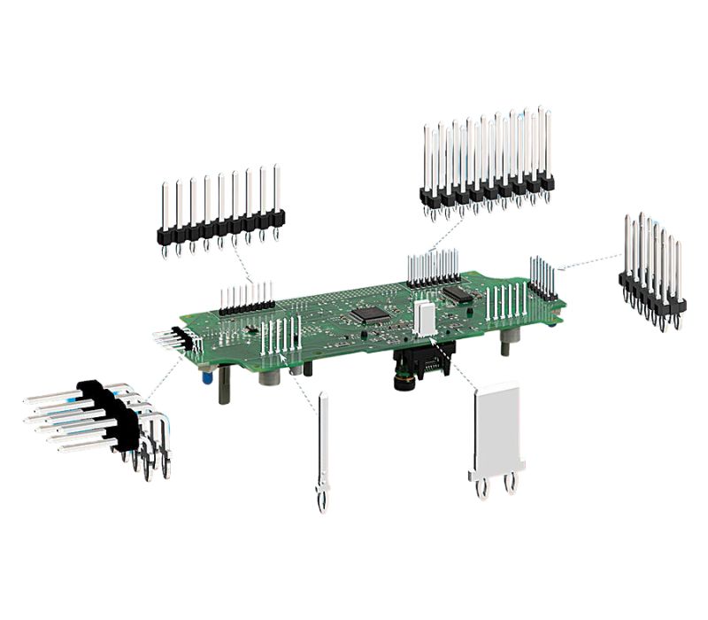
Boards are manufactured with minus side tolerance to hold connector / components with plating process control. Contact Us
To handle high current PCBs boards are manufactured for more than 105 microns & above. Contact Us
We offer Via filled with Silver conductive ink for Via in Pad PCBs for Planarize high dense PCBs for BGA / SMD. Contact Us
Specific Blind via connections inner layer to outer layer with Burier via connections restricts to only inner layers Contact Us
Fast turn PCB boards manufactured as per the customer time bound delivery for their critical assured delivery with good quality Contact Us
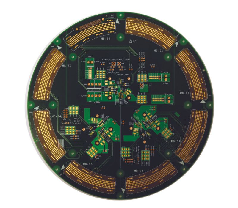
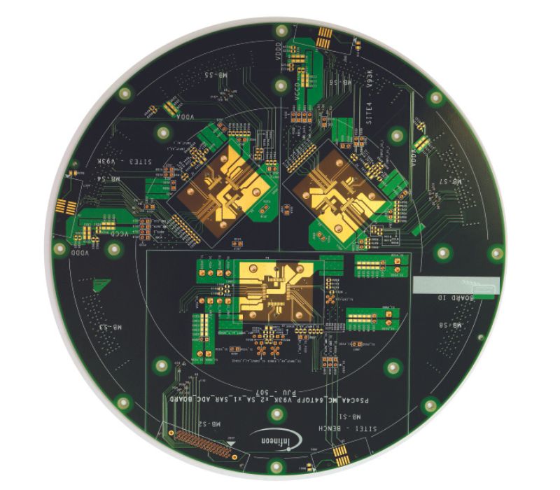
PCBs are used for satellite communication, control & navigation systems for unmanned Arial Vehicles. Contact Us
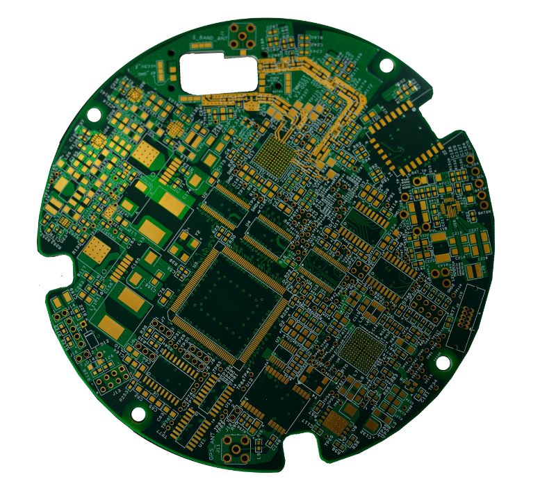
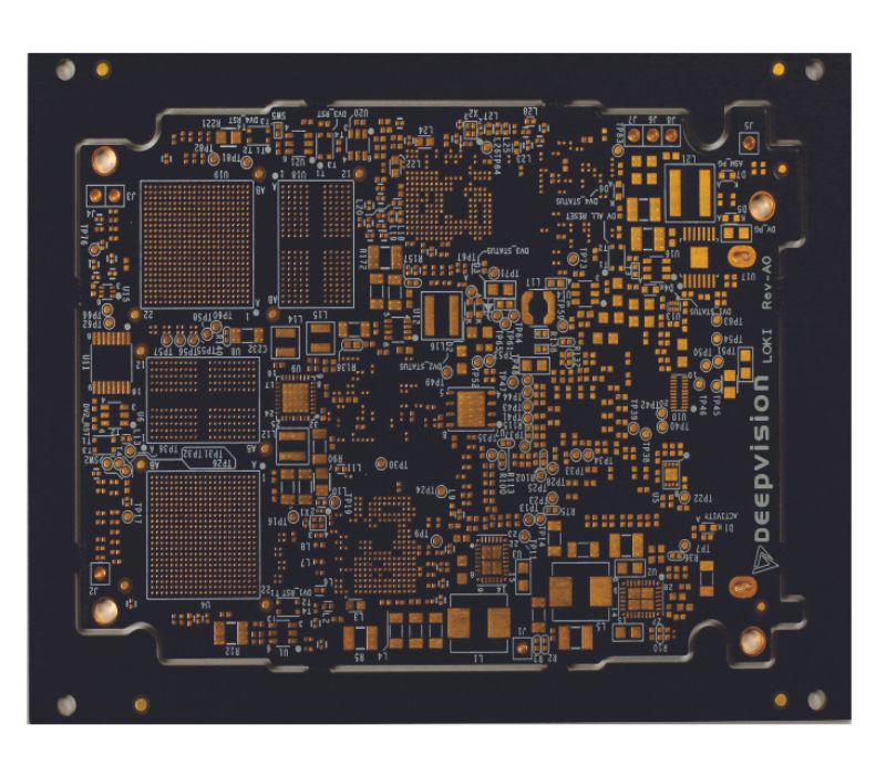
In-House manufacturing plant to manufacture Hi-end Multilayer PCBs Contact Us
Welcome to WordPress. This is your first post. Edit or delete it, then start writing!